 language
BGA Assembly Service, No MOQ
BGA assembly has become the heart of modern electronic packaging. In today’s high-speed, compact world, every millimeter of PCB space counts, and every signal must travel cleanly. That’s where Ball Grid Array (BGA) assembly steps in — a packaging method built for performance, precision, and reliability.
From smartphones and laptops to advanced automotive modules and aerospace controls, BGA assembly supports technologies that demand faster data processing and stable thermal performance.
What is Ball Grid Array (BGA) Assembly?
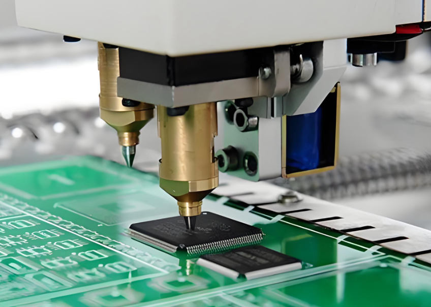
A Ball Grid Array, or BGA, is a surface-mount package that connects integrated circuits (ICs) to the PCB through tiny solder balls arranged in a grid pattern under the component. Instead of traditional leads or pins, BGAs use small solder balls arranged in a grid on the underside of the chip. During the reflow process, these solder balls melt, creating secure electrical and mechanical bonds between the IC and the board.
During assembly, these solder balls melt in a controlled reflow process, bonding the component to the circuit board. Compared to older packages such as QFP or SOP, BGAs offer higher pin density and better electrical performance. This makes them a go-to choice for high-performance devices like processors, GPUs, memory modules, and FPGAs.
BGA Package Types
With the rapid advancement of integrated circuit (IC) technology, the requirements for IC packaging have become increasingly stringent. When the operating frequency of an IC exceeds 100 MHz, traditional packaging methods can lead to a phenomenon known as crosstalk. Moreover, when the number of IC pins exceeds 208 pins, conventional packaging becomes more challenging to implement.
As a result, besides the QFP (Quad Flat Package) method, most high-pin-count chips today have adopted BGA (Ball Grid Array Package) technology. There are many different BGA package types are used depending on the application, performance, and cost requirements. Here are the main categories:
1. PBGA (Plastic BGA)
Usually constructed from 2–4 layers of organic material, forming a multilayer board. Intel’s Pentium II, III, and IV processors all used this type of packaging. In recent years, another variation has appeared — where the IC is directly bonded onto the substrate. This approach is much cheaper than standard PBGA packaging and is typically used in products with lower quality requirements, such as gaming devices.
2. CBGA (Ceramic BGA)
This refers to a ceramic substrate, where the electrical connection between the chip and substrate is typically achieved through a flip-chip (FC) mounting method. Intel’s Pentium I, II, and Pentium Pro processors all utilized this form of packaging.
3. FCBGA (Flip-Chip BGA)
A rigid multilayer substrate designed for high-performance applications.
4. TBGA (Tape BGA)
Uses a tape-based flexible substrate, generally consisting of 1–2 layers of PCB circuitry.
5. CDPBGA (Cavity Down PBGA)
Refers to a package structure with a square recessed cavity in the center area, also known as a cavity-down region, where the chip is placed.
6. Micro BGA (μBGA)
Designed for miniaturized electronics like smartphones and wearable devices, micro BGAs feature a very fine pitch and extremely small form factor.
7. Fine-Pitch BGA (FBGA)
FBGA has closely spaced solder balls, enabling higher connection density and improved electrical performance, commonly used in DRAMs and high-speed devices.
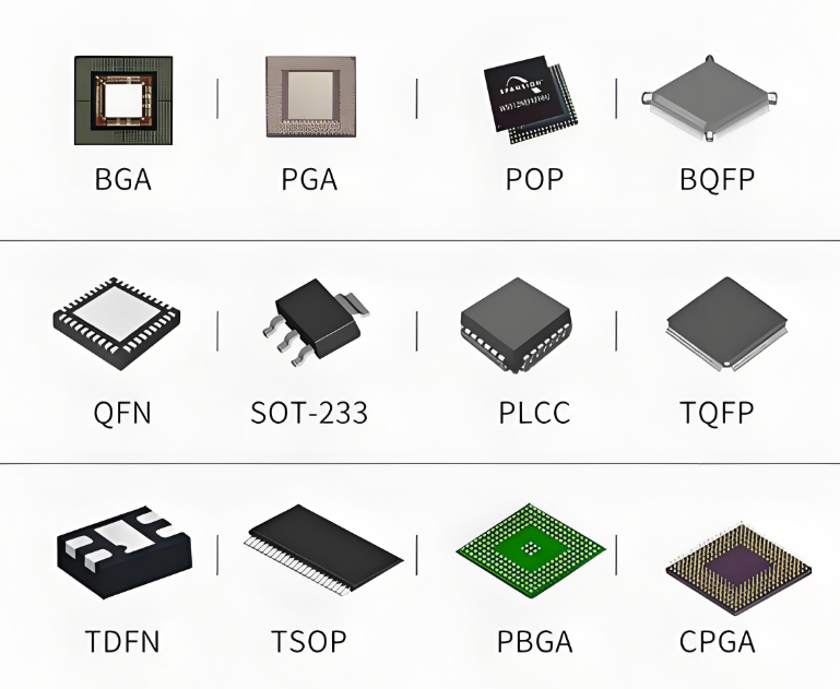
Each type offers a different balance of cost, durability, and performance. Selecting the right one depends on the specific application and environmental demands.
How Does a BGA Work?
In BGA packaging, each solder ball serves as both a mechanical support and an electrical pathway. When the assembly undergoes reflow soldering, the solder balls melt and bond with corresponding pads on the PCB.
This process forms short and uniform electrical paths between the chip and the board. The shorter paths reduce electrical resistance and inductance, enhancing the signal transmission speed. Additionally, the arrangement of solder balls under the chip allows for better heat distribution and dissipation, ensuring the component runs cooler.
After cooling, the solder solidifies, creating strong joints that can endure mechanical stress and thermal cycling.
Advantages of BGA Assembly
- Supports a large number of connections within a small footprint to integrate complex chips without expanding board size.
- Shorter interconnections minimize parasitic effects, reducing noise and improving high-speed signal integrity.
- The array of solder balls allows heat to spread more evenly, which is vital for processors and other heat-generating components.
- Since the solder joints are spread across the bottom surface, the component is mechanically stable and less prone to lead damage.
- BGAs save board space and reduce mechanical stress on solder joints, resulting in a longer product lifespan.
PCB Design Considerations for BGA
Designing a PCB for BGA assembly requires precision and foresight. Every pad, via, and trace must be carefully planned to guarantee manufacturability and reliable soldering. Here are a few essential points engineers always consider:
- Pad Design and Alignment:
The pad layout on the PCB must perfectly match the BGA ball pattern. Even the slightest misalignment can cause opens or bridging after reflow.
- Via-in-Pad Technology:
To save routing space and improve electrical performance, many designs use vias directly within pads. This allows signal traces to escape from dense BGA areas more easily.
- Solder Mask and Clearance:
Proper solder mask definition helps prevent short circuits between solder balls during reflow. Mask-defined pads are often preferred for fine-pitch BGAs.
- Thermal Balance:
Since BGAs generate heat, thermal vias and multiple copper layers are often added to improve heat dissipation and prevent warping.
- Inspection Accessibility:
Designers should leave enough space for X-ray inspection, as BGA joints cannot be visually inspected once soldered.
The goal in design is to create a PCB layout that supports strong solder joints, stable temperature performance, and high assembly yields. Even small design optimizations — such as pad diameter or stencil thickness — can make a significant difference in long-term reliability.
Best Technology Circuit’s BGA Assembly Capabilities
At Best Technology, BGA assembly is not just a process — it’s a craft refined through engineering precision and consistent quality control. We specialize in handling fine-pitch and micro BGA components, where even a single micron matters.
Our SMT lines are equipped with automated pick-and-place systems featuring high-resolution vision alignment. Each reflow oven is programmed with a custom thermal profile to suit the specific BGA package type, whether it’s PBGA, CBGA, or FBGA. Our engineers continuously monitor temperature zones to avoid overheating or warpage, ensuring every component settles precisely into position.
| Capability | Standard / Specification |
|---|---|
| Types of BGA | – Plastic Laminate BGA (PBGA) – Tape Ball Grid Array (TBGA) – Ceramic Ball Grid Array (CBGA) – Flip Chip Ball Grid Array (FCBGA) – Enhanced Ball Grid Array (EBGA) – Micro BGA- Package on Package (PoP) – Chip Scale Package (CSP) – Wafer Level Chip Scale Package (WLCSP) – Land Grid Array (LGA) – Column Grid Array (CGA) |
| BGA CSP Capability | – Package Size: 5mm × 5mm to 45mm × 45mm – Min. Solder Ball Pitch: 0.3mm / 0.5mm – Min. Solder Ball Diameter: 0.15mm / 0.25mm – Min. Solder Ball Height: 0.25mm – Max BGA Component Weight: 150g – Component Placement Accuracy: ±0.03mm |
| Chip Package Support | – BGA / LGA / HDA / POP / uBGA / WLCSP / CSP / CGA |
| Solder Paste Printing | – Stencil Thickness: 0.10mm – 0.15mm – Type: Laser-cut Stainless Steel / Nickel Electroformed – 3D SPI for paste height and volume control |
| Pick & Place Accuracy | – Placement Tolerance: ±25μm (fine-pitch BGA) – Machine Vision Alignment: Fiducial and Ball Recognition – Component Range: 01005 to 50×50mm |
| Reflow Soldering | – 10-zone Controlled Reflow Oven – Nitrogen Atmosphere Reflow Available – Custom Temperature Profiling for Each Package Type – Max Reflow Temp Tolerance: ±1.5°C |
| Quality Assurance | – Automated Optical Inspection (AOI) – X-ray Inspection (2D / 3D AXI) – Functional Testing (ICT / FCT) – Thermal & Mechanical Stress Testing – First Article Inspection (FAI) Report Available |
| BGA Rework & Repair | – PCB Reballing and Component Reballing – BGA Site Cleaning & Pad Restoration – Replacement of Damaged or Missing Solder Balls – Component Removal and Reinstallation – Controlled Rework Station with Localized Heating Profile |
| Inspection & Testing Equipment | – 3D X-ray System for Void Analysis – Solder Joint Cross-section Analysis – In-Circuit and Boundary Scan Testing – Real-Time Process Monitoring & SPC |
| Engineering & Documentation | – DFM (Design for Manufacturability) Review – DFA (Design for Assembly) Review – Custom Reflow and Stencil Design – Full Process Traceability via MES System |
| Certifications | – ISO 9001, ISO 13485, IATF 16949, AS9100D – IPC-A-610 Class 2 & 3 Standards – RoHS and REACH Compliant |
BGA Chips Assembly Process at Best Tech – Flow Chart
The assembly of BGA chips involves multiple controlled stages — each one critical to achieving consistent results. Below is a flow chart of BGA chips assembly process in Best Tech:
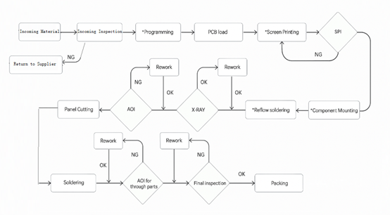
Here’s how key process flows in Best Technology:
1. Solder Paste Printing:
It all starts with the stencil printing step. We use stainless steel or laser-cut stencils to deposit the exact amount of solder paste onto each pad. Proper alignment here is crucial because it directly influences solder joint shape and volume.
2. Automated Component Placement:
Next, BGA components are placed using advanced pick-and-place equipment with vision-assisted correction. The system identifies fiducial marks and ensures the BGA sits perfectly centered on its pads.
3. Reflow Soldering:
During reflow, the board passes through temperature-controlled zones inside the oven. The solder balls melt and then solidify as the board cools, forming perfect dome-shaped joints under the package. Our reflow profiles are precisely tuned for each BGA type, balancing soak, peak, and cooling times.
4. Inspection and Verification:
After reflow, all boards undergo Automated Optical Inspection (AOI) for surface components and 3D X-ray scanning for BGAs. The X-ray images show details like solder ball shape, void percentage, and any misalignment, ensuring that every board meets our quality benchmarks.
5. Functional Testing:
When requested, we also perform functional and in-circuit testing (ICT) to validate that all BGA connections perform correctly under real operating conditions.
How to Ensure Good Soldering in BGA Assembly?
Consistent soldering quality depends on multiple controlled factors. At Best Technology, every stage — from paste printing to reflow — is tightly monitored to secure the best possible solder results. Here we some ways that we performed in process to ensure highest quality of BGA assembly:
- Use fresh, high-quality solder paste with correct alloy composition.
- Maintain uniform paste thickness to ensure all joints have equal solder volume.
- Control reflow temperature profiles with accurate preheat, soak, and cooling stages.
- Use a nitrogen-controlled reflow environment to reduce oxidation.
- Prevent PCB contamination—any residue can interfere with wetting.
- Use moisture-sensitive packaging for components to prevent reflow damage.
- Conduct X-ray inspection after each production batch.
Combining these controls leads to stable, durable joints capable of withstanding thermal cycling, vibration, and aging. This is why our BGA assemblies perform reliably across demanding sectors — from aerospace and automotive to industrial control.
Applications of BGA Assembly
BGA technology is widely used across industries due to its compactness and performance advantages:
- Computing and Servers: CPUs, GPUs, and memory modules.
- Consumer Electronics: Smartphones, tablets, and smartwatches.
- Automotive Electronics: Engine control units (ECUs), sensors, and infotainment systems.
- Medical Devices: Portable diagnostic and monitoring equipment.
- Aerospace and Defense: Avionics systems requiring vibration and thermal stability.
Wherever reliability and density matter, BGA assembly is a preferred solution.
Common FAQs about BGA assembly
1. What is the typical lead time for BGA assembly?
Lead time depends on project complexity, but standard prototype runs take 7–15 working days, while production runs range from 2–4 weeks.
2. What is the smallest BGA pitch you can assemble?
At Best Technology, we can assemble BGAs with pitches as small as 0.3mm, using high-precision optical alignment and X-ray inspection.
3. Do you perform 100% X-ray inspection for BGAs?
Yes, all BGA assemblies are 100% X-ray inspected to ensure accurate solder joint formation and alignment.
4. Can you handle BGA rework or reballing?
Yes, we provide BGA rework and reballing services, ensuring defective assemblies can be corrected without damaging the PCB.
5. What factors affect the quality of BGA assembly?
Key factors include solder paste quality, reflow profile accuracy, board warpage, component moisture level, and inspection consistency.